
Working as an IT reporter gave me the chance to learn about new technologies and AI developments before many others. That was also true when ChatGPT appeared in late 2022. I introduced it to people around me, but the response was lukewarm.
“What is that?” “AI isn’t very accurate.” “I’ll try it when it becomes commercially available.”
Nearly four years have passed since then. Students now use AI for assignments, office workers use ChatGPT to write reports, and companies are pursuing “AI transformation” (AX), changing their organizations and ways of working.
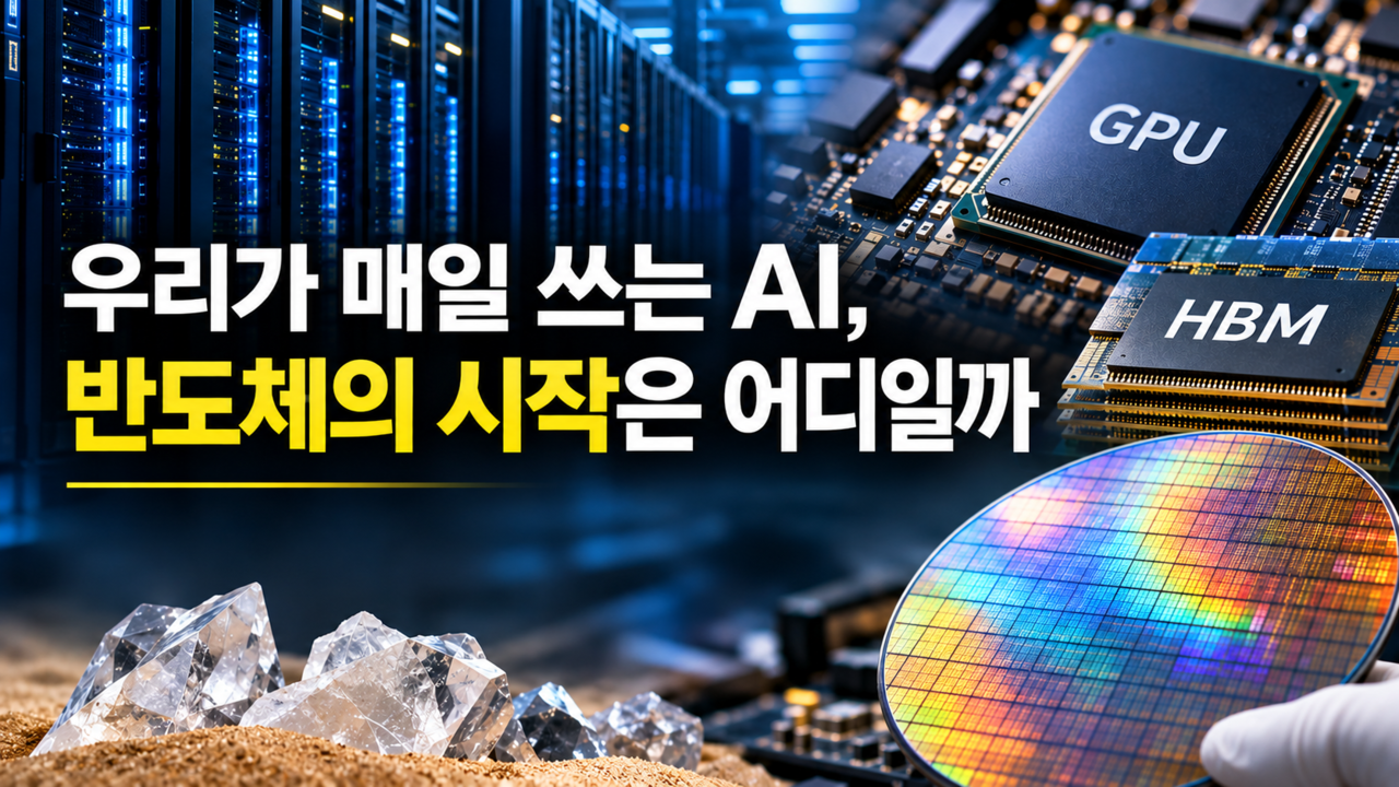
I found myself wondering how this kind of AI is made. Not all the computing takes place inside a smartphone. The questions we send travel over the internet to data centers. The servers installed there contain Nvidia GPUs and HBM produced by companies such as SK hynix and Samsung Electronics. HBM is high-performance memory made by stacking multiple layers of DRAM. DRAM is manufactured on silicon wafers.
Interestingly, the semiconductor market was in a downturn when ChatGPT appeared. Demand for PCs and smartphones slowed during the COVID-19 pandemic, pushing memory chip prices down. Samsung Electronics and SK hynix also suffered weaker results.
But the rapid spread of generative AI changed the situation. Data-center investment grew, and demand surged for GPUs and HBM, which are needed for AI computing.
In November 2024, SK Group Chairman Chey Tae-won forecast that the AI market could expand significantly around 2027, driven by the arrival of next-generation ChatGPT models.
How is AI connected to the vast semiconductor industry? Starting with ChatGPT, I traced the chain backward all the way to sand, a raw material for semiconductors.
1. AI services (the AI we use every day)

ChatGPT, Google Gemini, and Anthropic’s Claude are leading generative AI services.
When users enter a question, an AI model processes it and generates a response. AI can also write text and translate languages. Some AI services generate images and videos as well.
Not all AI computing takes place in the chat window we see. When we enter a question, it is sent to a server over the internet. The AI model generates an answer on the server, then sends the result back to the user.
Some AI features can, of course, run on smartphones or PCs. But large-scale generative AI services generally process their computing workloads in data centers.
2. AI companies (who makes AI models?)
ChatGPT was created by the U.S. company OpenAI. Google developed Gemini, and Anthropic made Claude. Meta and Chinese AI companies are also developing their own models.
AI companies train their models using vast amounts of data. When users ask questions, the trained models generate responses.
This process is broadly divided into training and inference. Training is the process by which an AI learns patterns from data. Inference is the process by which a trained model answers questions or creates new results. When we ask an AI a question and receive an answer, that is primarily inference.
Both training and inference require extensive computing. Developing large-scale AI models in particular demands enormous computing power. That is why AI companies are investing heavily in data centers and high-performance semiconductors.
3. Data centers (where AI actually operates)

A data center is a facility that houses and operates large numbers of servers. From the outside, it looks like a large building. Inside, rows of equipment racks hold the servers. The facility also has power systems and cooling equipment to remove heat.
AI companies train models and run services in data centers. They may use their own facilities or rent computing resources from cloud providers.
Training large-scale AI models requires many semiconductors to operate at the same time. Running services also requires enough computing power to handle requests from many users.
Power and heat are major challenges. The more high-performance semiconductors operate, the more electricity they consume. They also generate substantial heat, making cooling systems essential.
As the AI market grows, securing power and developing cooling technology are becoming major challenges alongside data-center construction.
4. Servers (the computers that power AI)
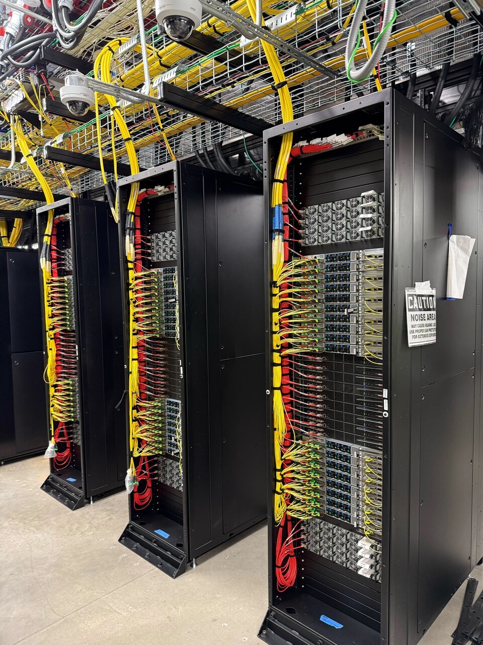
A server is, at its core, a computer. Like the PCs we use, it processes calculations and stores data. The difference lies in its purpose and scale.
While a personal computer is designed for one person, a server is built to handle requests from many users.
Servers contain CPUs, memory, and storage. Servers used for AI computing also use accelerators such as GPUs. A CPU manages the computer as a whole and handles a wide range of instructions. AI accelerators perform large-scale calculations quickly.
Connecting multiple servers makes it possible to train larger AI models or handle requests from many users at once. However, not every AI accelerator is installed in a conventional server. In some cases, multiple chips are connected in dedicated systems, as with Google’s TPU.
What matters in an AI system is how many calculations it can perform, and how quickly. This is where GPUs and TPUs come in.
5. GPUs and TPUs (the semiconductors responsible for AI computing)
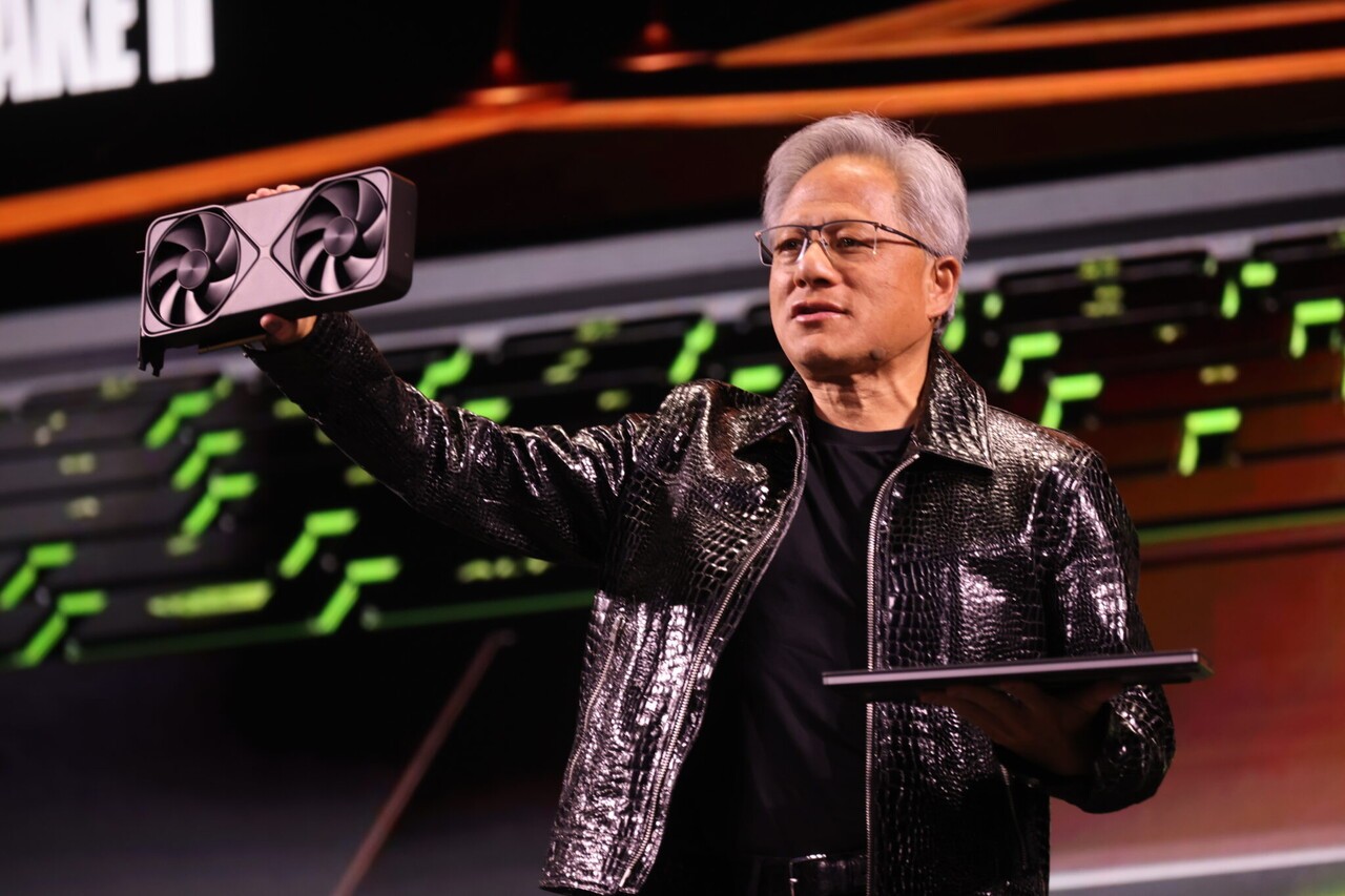
AI requires an enormous number of calculations. Semiconductors that perform this work quickly are called AI accelerators.
Leading examples include Nvidia GPUs and Google TPUs. GPU stands for Graphics Processing Unit. GPUs were originally developed to process graphics for games and video. Their ability to perform many calculations simultaneously has also made them widely used for AI training and inference.
Nvidia has developed GPUs for AI computing. By also providing related software and systems, it has secured a strong position in the AI semiconductor market.
Google chose a different path, developing its own TPU specifically for AI computing. TPU stands for Tensor Processing Unit. These semiconductors are designed to quickly perform the large matrix calculations repeated in AI models. Google uses TPUs in its own AI services and cloud infrastructure.
GPUs and TPUs differ in their design goals and architectures. GPUs are used for a wide range of computing, from graphics to AI. TPUs are specialized for the calculations required in machine learning.
They also have something in common: both must process large amounts of data quickly. No matter how fast a processor is, it cannot perform to its full potential if the data it needs is not supplied in time. This is where HBM comes in.
6. HBM (memory that supplies data to AI accelerators)
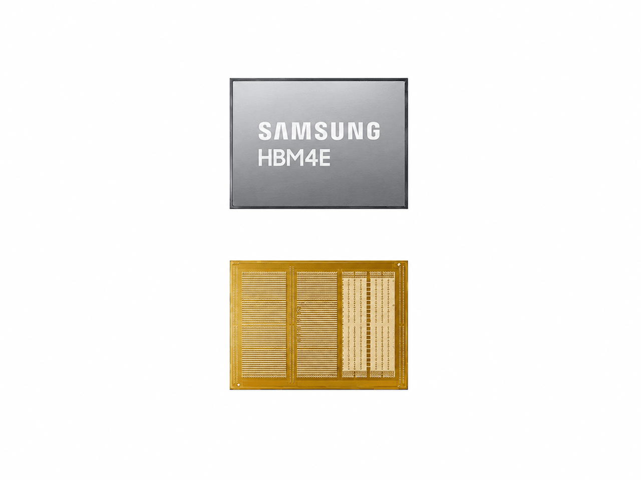
HBM stands for High Bandwidth Memory. Put simply, it is memory designed to transfer large amounts of data at once and at high speed.
Why does AI need memory? GPUs and TPUs handle calculations, while memory stores the data needed for those calculations. Memory holds the many numbers that make up an AI model as well as the data generated during computation. An AI accelerator reads this data, performs calculations, and writes the results back to memory.
Speed is the challenge. AI accelerators process enormous amounts of data in a short time. If memory cannot supply data quickly enough, the processing unit has to wait. In other words, even a fast GPU cannot perform to its full potential.
HBM was developed to reduce this problem. Multiple DRAM chips are stacked vertically and connected to one another, allowing large amounts of data to be transferred simultaneously.
Using advanced packaging technology, HBM is positioned close to AI accelerators such as GPUs. This shortens data-transfer distances and provides high bandwidth. Google TPUs also use HBM, depending on the product.
SK hynix, Samsung Electronics, and U.S.-based Micron are leading HBM manufacturers. The spread of generative AI has driven a sharp increase in demand for HBM.
7. DRAM (the basic semiconductor used to make HBM)
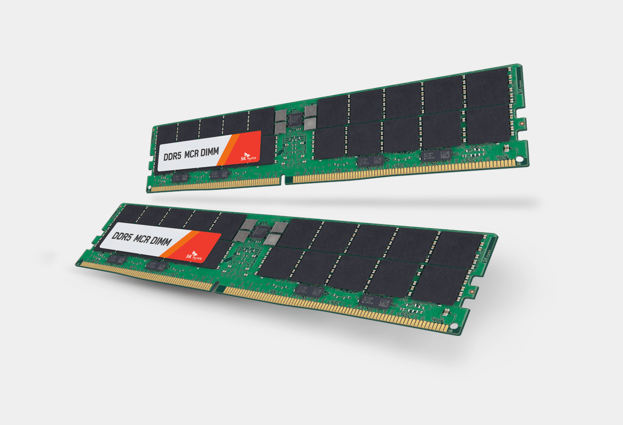
DRAM stands for Dynamic Random Access Memory.
It is a semiconductor that temporarily stores the data a computer needs while it is working. DRAM is used for tasks such as editing documents and running programs.
When the power is cut, data stored in DRAM disappears. Its function is different from that of storage devices, which keep photos and files for long periods.
HBM is also based on DRAM technology. Multiple DRAM chips are stacked vertically and connected through tiny pathways that allow them to exchange data. One key technology used in this process is TSV.
TSV stands for Through-Silicon Via. It is an electrical connection pathway that passes vertically through a silicon chip. This technology enables data to move quickly between stacked memory chips.
How is DRAM made? DRAM is also a type of semiconductor. First, numerous circuits are created on a thin, round disc. After inspection, the disc is cut into small chips. The round disc used in this process is called a wafer.
8. Wafers (the round discs used to make semiconductors)
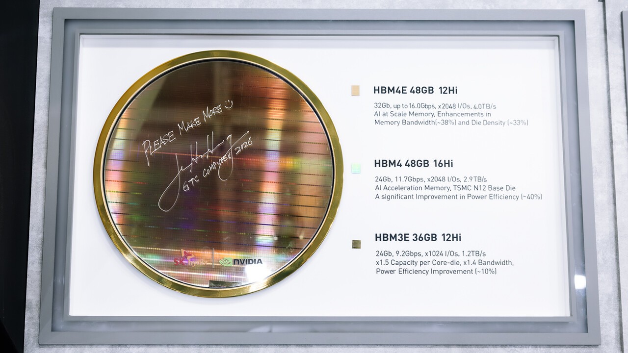
The thin, round discs often seen in photos of semiconductor factories are wafers.
Semiconductors, including DRAM, are made by etching fine circuits onto these wafers. Multiple semiconductor chips can be produced from a single wafer.
The main material used to make wafers is silicon. Its chemical symbol is Si. The silicon used in semiconductors is refined to a high level of purity, removing even minute impurities.
The refined silicon is processed into thin discs, and circuits are formed on them. The wafers are then inspected and cut into individual chips, which are packaged. Where does the silicon used to make wafers come from?
9. Sand and quartz (tracing semiconductor materials back to their source)

Silicon is a relatively common element. Sand and quartz contain silicon dioxide (SiO₂), a compound of silicon and oxygen. In the semiconductor industry, silicon is obtained mainly from suitable raw materials, such as high-purity quartz.
The raw material is first processed to produce silicon. Impurities are then removed to refine it to the high purity required for semiconductor manufacturing. A single crystal is grown from the refined silicon, then sliced into thin wafers.
DRAM is made on these wafers. Stacking multiple layers of DRAM creates HBM. HBM supplies data to AI accelerators such as GPUs and TPUs.
AI accelerators are used in data centers to train models and generate responses. Those results reach us through the AI services we use.
Of course, you cannot scoop up beach sand and use it to make a semiconductor directly. Silicon for semiconductors must go through rigorous refining and manufacturing processes.
Finally: How AI has changed the semiconductor industry
The spread of generative AI is changing the structure of demand in the semiconductor market. AI has emerged as a new engine of growth in a memory chip market that had been centered on PCs and smartphones.
As AI models become more advanced, demand is rising for AI accelerators such as GPUs and TPUs. HBM, which rapidly supplies the data required for large-scale computing, has also become a key semiconductor.
Growth in the AI industry is driving investment not only in semiconductors, but also in servers, networking equipment, and power and cooling infrastructure. The expansion of AI services is affecting industries across the board.
I hope this article has been a small help in understanding AI and semiconductors—subjects that are familiar to us but can feel difficult to grasp.