
Key points
The 28th SEDEX opened at COEX in Seoul on October 14. The record-breaking event features 888 booths operated by 300 companies through October 16.
Samsung Electronics displayed a model of “zHBM,” which stacks HBM on top of an AI accelerator. SK hynix presented its “HBF” concept, which uses NAND to target roughly 10 times the capacity of HBM from the same generation.
Both technologies are next-generation architectures still under development. Their status should be distinguished from that of HBM4E, for which Samsung has supplied samples to customers.
South Korea’s largest semiconductor exhibition, the 28th Semiconductor Exhibition (SEDEX 2026), opened at COEX in Seoul on October 14.
Hosted by the Korea Semiconductor Industry Association, this year’s event runs for three days through October 16. Around 300 companies—70 more than last year—have set up 888 booths.
Samsung Electronics and SK hynix are looking beyond the competition over HBM performance, putting the spotlight on technologies designed to reduce data-flow bottlenecks within AI systems.
A new tier between memory layers
In a keynote address titled “The Evolution of Memory Technology in the AI Era,” Ahn Hyun, SK hynix’s chief development officer, said, “As the AI inference market grows, data movement between memory tiers is emerging as a new performance bottleneck.” He added, “New tiers will be inserted between existing memory layers to meet a range of performance and capacity requirements.”
A memory hierarchy organizes different types of memory and storage according to how frequently data is used and how quickly it needs to be processed.
In the past, the challenge was to standardize a hierarchy running from SRAM and DRAM to SSDs and network storage. But the rapid rise in demand for AI computing has increased the role of HBM. The next step, he explained, will be to add new types of memory between existing tiers and optimize their functions to meet customers’ specific speed and capacity requirements—a concept known as custom memory.
Samsung combines packaging and foundry services with HBM4E
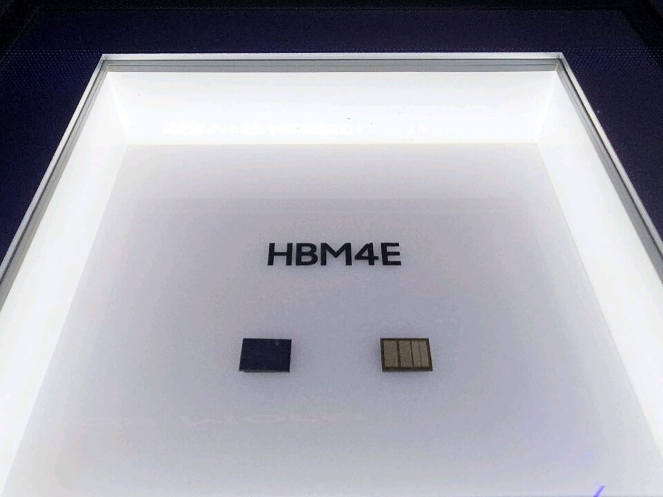
Samsung Electronics brought memory, system semiconductors and foundry services together in a single booth under the theme “AI System Design.” At the center was HBM4E, the seventh generation of HBM.
The product, whose first 48GB 12-layer samples shipped in May, uses 1c DRAM and a 4-nanometer logic die. It offers speeds of up to 16 Gbps per pin and bandwidth of up to 3.6 TB/s per stack. Compared with HBM4, its operating speed is more than 20% higher and its energy efficiency more than 16% better.
Samsung also displayed a model of “zHBM,” a three-dimensional architecture that brings memory and processing units closer together. Instead of placing HBM beside an AI accelerator, the design stacks it vertically above the accelerator to shorten data-transfer distances.
Other exhibits included LPDDR-PIM, which performs some computations within memory, and zNAND-O, which stacks NAND in four or eight layers. In packaging, Samsung showed “2.3D Cube-E,” which uses an RDL interposer instead of a silicon interposer; “3D Cube-H,” which vertically stacks a GPU and HBM using hybrid bonding; and a CPO model that connects chips using optical signals.
The goal is to improve AI system efficiency by integrating not only memory performance but also manufacturing and connectivity technologies.
SK hynix proposes a new memory tier with NAND-based HBF
Alongside HBM4E, the SK hynix booth featured models of HBM and high-bandwidth flash (HBF) architectures. Unlike HBM, which stacks DRAM, HBF vertically stacks NAND flash, taking advantage of its suitability for high-capacity storage.
SK hynix is targeting half the bandwidth and about 10 times the capacity of HBM from the same generation. The company envisions HBF as a new memory tier between HBM and storage devices, handling data needed for large-scale AI inference.
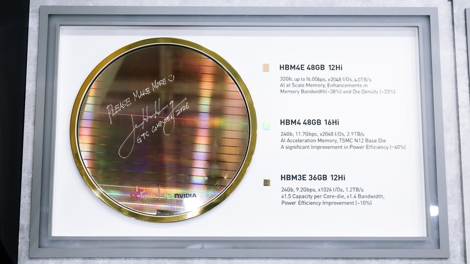
The booth also featured an HBM wafer signed by Nvidia CEO Jensen Huang, an exhibition on the history of HBM development, 256GB 3DS RDIMMs, 128GB MRDIMMs and 64GB 1c RDIMMs for AI servers, liquid-cooled enterprise SSDs, GDDR7, LPDDR6 and UFS 5.0.
Equipment and materials makers compete in advanced packaging
Materials, components and equipment companies also highlighted advanced packaging. Jusung Engineering introduced its atomic layer growth (ALG) technology, which it says it was the first in the industry to implement.
Hanmi Semiconductor showcased its “TC Bonder 4” for HBM4 production, a wide TC bonder scheduled for release next year, cutting, cleaning and placement (MSVP) equipment, and five types of 2.5D packaging equipment. Dongjin Semichem put the spotlight on DJBF, a packaging build-up film it has localized after the market had been dominated by Japan.
PSK and PSK Holdings displayed products spanning front-end and back-end processes, from plasma-based photoresist stripping, dry cleaning and etching equipment to fluxless reflow and descum equipment for HBM. SEMES, Samsung Electronics’ equipment subsidiary, presented products ranging from cleaning and etching equipment to bonders and probers.
International conferences on advanced packaging research and development, a global semiconductor standards forum, and a semiconductor market outlook seminar will also take place during the event.