
In brief
▶ On November 1, Samsung Electronics Chairman Lee Jae-yong visited the company’s Advanced Package Lab (APL), a research center for advanced semiconductor packaging in Yokohama, Japan, to review research into next-generation packaging technologies.
▶ Lee reviewed the development of materials and process technologies for advanced packaging with APL researchers and discussed ways to work with Japan’s materials, components and equipment industries. He urged them to secure advanced packaging technologies that will determine semiconductor competitiveness in the AI era.
▶ Samsung Electronics established the APL in Yokohama in 2023 and is investing 40 billion yen (about 350 billion won) over five years starting in 2024 to build a research base in Japan.
▶ The APL develops and validates materials and process technologies needed for advanced packaging. It serves as a link between Samsung Electronics’ semiconductor design and manufacturing capabilities and Japan’s materials, components and equipment ecosystem.
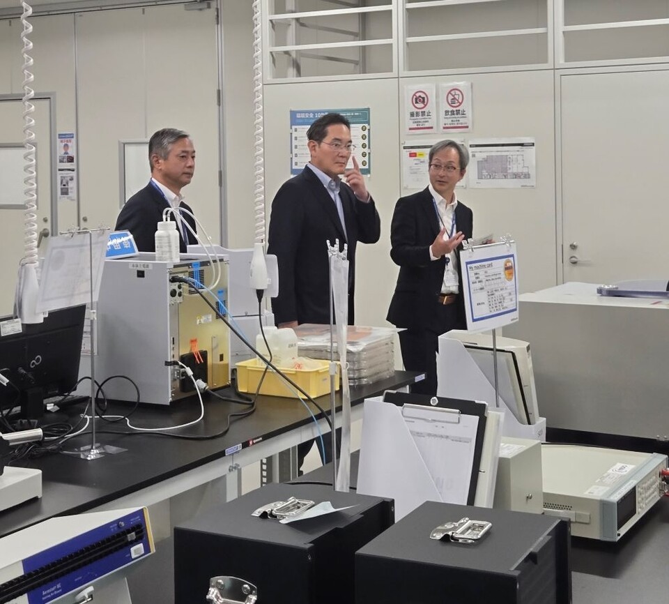
Samsung Electronics Chairman Lee Jae-yong visited the company’s semiconductor research center in Japan. On November 1, Lee went to the Advanced Package Lab (APL), an advanced semiconductor packaging research center in Yokohama, to review research into technologies for next-generation packaging.
Lee reviewed the development of materials and process technologies for advanced packaging with APL researchers and discussed collaboration with Japan’s materials, components and equipment industries. He also urged the team to secure advanced packaging technologies that will determine semiconductor competitiveness in the AI era. The APL officially opened on September 8, and Lee’s visit was its first review by the chairman, about two months after its opening.
◆ 40 billion yen over five years
Samsung Electronics established the APL in Yokohama in 2023 to research packaging technologies. Since 2024, it has been investing 40 billion yen (about 350 billion won) over five years to build a research base in Japan.
The APL develops and validates component technologies, including materials and processes, required for advanced semiconductor packaging. It serves as a bridge between Samsung Electronics’ semiconductor design and manufacturing capabilities and Japan’s strong ecosystem of materials, components and equipment technologies.
Alongside developing next-generation process and materials technologies such as wafer bonding and glass substrates, the APL is also expected to develop new high-performance packaging structures for mass-producing the low-power, high-performance semiconductors needed in the AI era.
Wafer bonding is a technology that stacks chips by directly joining wafers. Glass substrates use glass instead of conventional plastic substrates, enabling more signals to travel at higher speeds.
The APL will divide research areas with the packaging research organization under Samsung’s Korea-based semiconductor research institute, with the two teams working closely together to generate synergies. Samsung Electronics plans to continue expanding its local research workforce and develop Yokohama into a global R&D hub for next-generation packaging technologies.
◆ Yokohama
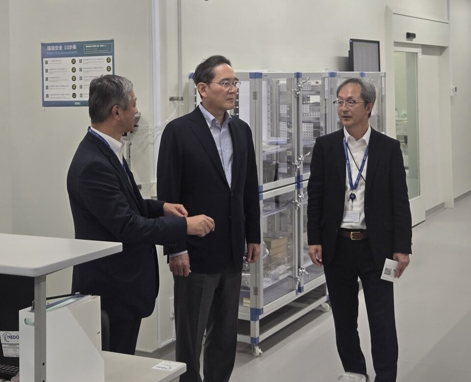
Samsung chose Japan for its ecosystem. The country has many companies with world-class expertise in semiconductor materials, components and equipment, as well as a well-developed industry-academia-research network that makes it a good place for technology partnerships and R&D.
The Japanese government has also designated semiconductors and AI as strategic sectors and is pursuing investment and support policies. Samsung Electronics said it views Japan as an attractive research base for semiconductor technology development and expanded local collaboration.
Yokohama, in particular, is a major city adjacent to Tokyo with many leading universities and research institutions, making it easier to recruit specialized researchers. Companies working on advanced packaging materials and equipment are also concentrated there, creating favorable conditions for collaboration.
Samsung Electronics plans to use Yokohama’s talent and industry-academia-research infrastructure to develop the APL into a hub for research collaboration linking Japanese materials and equipment companies with Samsung’s semiconductor expertise.
◆ The final stage of manufacturing: packaging
Advanced packaging is rapidly gaining importance as a key factor in AI semiconductor performance. Packaging is the final manufacturing stage, protecting chips and connecting them to external components.
In the past, packaging was mainly a way to encase a chip. Today, it has become a technology for combining multiple semiconductors—such as GPUs, HBM and accelerator chips—into a single package. The integration method directly affects bandwidth for data moving between chips, power efficiency and heat dissipation. In other words, even with the same chips, how they are combined can change the performance of an AI system.
Samsung Electronics said it will continue developing technologies to strengthen the competitiveness of next-generation products by securing key materials and equipment technologies needed for advanced packaging, in addition to its memory and logic semiconductor technologies.