Major companies such as Samsung, SK hynix and Celltrion announced plans on the 2nd to invest a total of 392 trillion won in advanced industries in the Chungcheong region.
The government responded with a special mega-zone designation and a seven-part support package. A pan-ministerial task force will be launched immediately to draw up a comprehensive plan within 100 days.
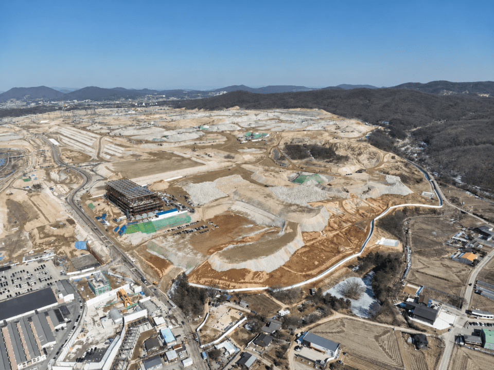
The Chungcheong region is emerging as a new hub for the semiconductor back-end process and materials-and-components industries. At the “National Report Meeting on Chungcheong Region Advanced Industry Development Vision” held in Asan, South Chungcheong Province on the 2nd, major companies including Samsung, SK hynix and Celltrion unveiled investment plans totaling 392 trillion won.
The announcement was a regional follow-up to the “three mega projects” revealed on the 29th of last month. It came after the Southwest region’s plan on the 30th of last month. By region, the amount is the second-largest after the Honam region’s 896 trillion won. The government will disclose the Yeongnam region plan in Jinju, South Gyeongsang Province on the 3rd.
What stands out more than the size is the composition of the investment. Chungcheong’s share is not focused on front-end processes that etch circuits onto wafers. Instead, it is weighted toward back-end processes that stack and connect chips to complete them, as well as materials and components such as displays, batteries and substrates. Analysts say this aligns with the direction in which the axis of semiconductor competition is shifting in the AI era.
Samsung’s 140 trillion won plan and SK hynix’s 100 trillion won plan outline the investment landscape in detail. Samsung Display President Lee Cheong said at the report meeting that the company will invest 67 trillion won in Asan displays, 56 trillion won in HBM (high-bandwidth memory) fabs in Onyang and Cheonan, 9 trillion won in batteries in Cheonan, and 8 trillion won in package substrates in Sejong.
SK hynix will invest about 100 trillion won in NAND flash and advanced packaging production facilities. Celltrion will invest 2 trillion won in biopharmaceutical production facilities. In addition, investments by other companies in AI data centers worth about 150 trillion won brought the total for the Chungcheong region to 392 trillion won.
SK hynix’s NAND investment also reflects a broader trend. As AI data centers expand, demand for large-capacity storage devices is rising as well. Analysts say this shows memory investment is broadening beyond a focus on DRAM to include NAND.
The venue itself carried symbolism. The report meeting was held at Samsung Display’s Asan campus, where the first glass substrate for mass production of 8.6-generation OLEDs was introduced. This is the world’s first attempt of its kind. The government’s choice of this location for the announcement is interpreted as an effort to brand the Chungcheong region as the cradle of “manufacturing technology.”
The biggest change in this plan is in Onyang. President Lee said, “The old Onyang package line was a process centered on assembly and testing,” adding that the existing line will be transformed into a next-generation fab to develop Onyang and Cheonan into a global HBM hub.
This statement encapsulates the shift in the semiconductor industry’s center of gravity. HBM is made by stacking DRAM vertically. How precisely chips are stacked and connected determines performance. That means back-end process technology has become as important a battleground as front-end circuit design. Packaging, once considered a low value-added process, has been elevated to an investment target on the level of advanced fabs.
Within the government’s national balanced development strategy, Chungcheong’s role has also become clear. The regional division of labor will place a second semiconductor cluster in Honam for front-end processes, packaging advancement in Chungcheong, and physical AI plus materials, components and equipment hubs in Yeongnam. In other words, each region will handle a different stage of the semiconductor value chain.
For Chungcheong, the plan matches its existing industrial base. This is because Asan and Cheonan already have display industries, Cheongju has semiconductors, and Osong has biopharmaceuticals. The assessment is that rather than introducing new industries, the plan is more about strengthening existing roots.
Infrastructure support will follow the industrial base. The government will build an advanced packaging R&D facility and a semiconductor gas performance and safety evaluation center in Chungcheong. It also plans to establish a display demonstration center, a battery fire safety evaluation center and a public biofoundry. The idea is not merely to attract production facilities, but to embed research, demonstration and safety infrastructure as well.
The core of the government’s support measures is the “Chungcheong Region Next-Generation Advanced Industry Promotion Strategy.” Its framework consists of a seven-part policy support package covering fiscal policy, finance, regulation, technology development, taxation, human resources and infrastructure. Mega-zones that ease complex regulations on companies will be designated, and the Growth Engine Special Subsidy and the National Growth Fund will also be mobilized.
The “Chungcheong Advanced Strategic Industry Leap Task Force,” involving the government, local governments and companies, has been launched immediately. It will provide integrated support for site selection, permitting, electricity, water, labor and financing issues, and will prepare a comprehensive support plan within 100 days. Minister of Trade, Industry and Energy Kim Jung-kwan said that day, “We will not stop at a declaration but will stand with companies to the end so this leads to tangible results.”
On the same day, companies, the central government and local governments in the Chungcheong region also signed investment agreements. The structure assigns companies responsibility for carrying out investments, while the government and local governments are responsible for building the ecosystem and resolving obstacles.
The remaining challenges are significant. Much of this investment is a long-term plan running through 2040. The business community estimates the national investment scale at 4,755 trillion won. That means the pace of implementation could fluctuate depending on the semiconductor cycle and broader economic conditions.
Securing electricity and water will also be a test. HBM fabs and AI data centers are representative high-power-consumption facilities. As large-scale investment announcements continue, concerns over fairness among regions have also emerged. President Lee Jae-myung said at a Cabinet meeting on the 30th of last month, “Regions that feel left out may be disappointed,” and added that additional measures would be prepared to address that.
392 trillion won is not the result, but the starting line. Only when the investment agreements signed that day lead to groundbreaking, and groundbreaking to mass production, will the Chungcheong vision take concrete shape. The comprehensive support plan due in 100 days is expected to be the first major test.