
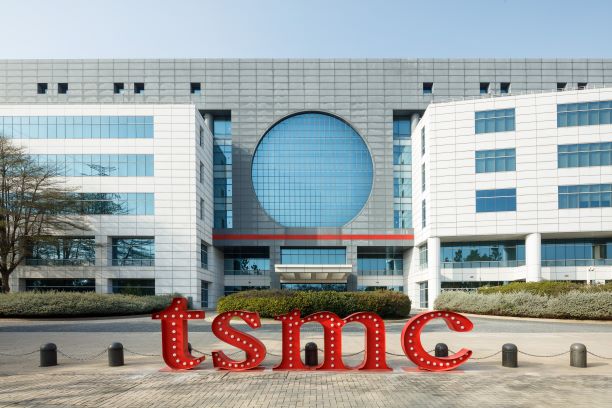
TSMC, Taiwan’s leading contract chipmaker, has pulled ahead in one of the key battlegrounds of next-generation semiconductor process technology: backside power delivery. According to the industry on the 18th, TSMC has completed the development and verification of its Angstrom-class A16 process, the first in the industry to apply Super Power Rail (SPR), a backside power supply method.
Angstrom is one-tenth of a nanometer. A16 is a 1.6-nanometer-class process, a technology that etches circuits down to a scale tens of thousands of times thinner than a human hair.
◆ Bringing the power path to a “underground road” on the back of the chip
Backside power technology is easy to understand by comparing it to roads. In conventional semiconductor chips, both the signal wiring that carries data and the power wiring that delivers electricity are laid on the same “front-side” road. It is like having pedestrian paths and freight lanes overlap.
As processes become more advanced, the road gets narrower even as the number of wires increases. The two wiring networks become tangled in a confined space, causing congestion. Electricity must take complicated routes, increasing resistance and lowering voltage. It is similar to how water pressure weakens when pipes become long and winding. In the industry, this is called IR drop, or voltage drop.
Backside power is a solution that moves the freight lane underground. It shifts the power wiring entirely to the back of the chip and leaves the front-side road for signal wiring only. Electricity can then be supplied more stably through a thicker, straighter path, while signals travel smoothly on widened lanes without congestion.
◆ Where TSMC moved ahead
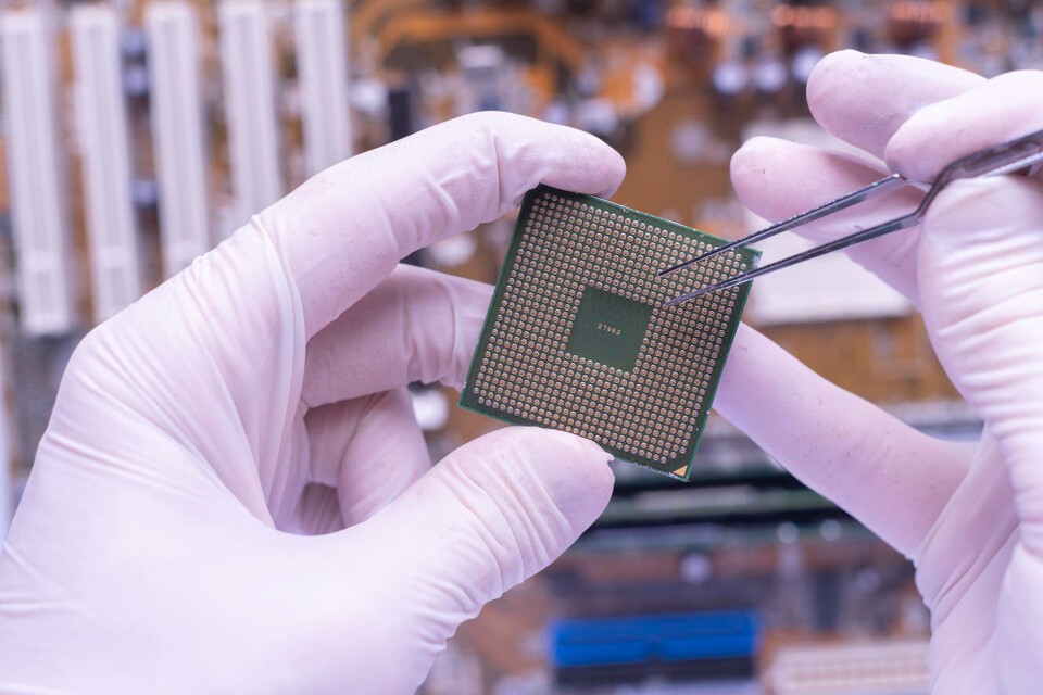
The challenge lay in the construction method. To draw power from the backside, manufacturers typically have to significantly redesign transistor placement and cell structures. That creates the burden of giving up part of the cell libraries and design know-how accumulated over years, the basic building blocks of semiconductor design.
TSMC found a way to reduce that burden. Through a dedicated contact structure, it directly connects power to each transistor’s source and drain while leaving the front-side gate structure, cell size, and placement area almost unchanged.
The key achievement is that it preserved the gate density and design flexibility of its existing N2P process. For customers, that means they can move to the new process without major changes to existing design assets.
The performance gains were also quantified. Compared with N2P, speed improves by 8% to 10% at the same power, or power consumption drops by 15% to 20% at the same speed. Chip density also increases by 8% to 10%. The combination is considered especially well suited for AI and high-performance computing (HPC) chips, where complex signal paths and dense power networks are essential. Mass production of A16 is scheduled to begin in the fourth quarter of this year, and foreign media have reported that Nvidia may adopt A16 for its next-generation GPUs.
◆ A three-way race with Intel and Samsung
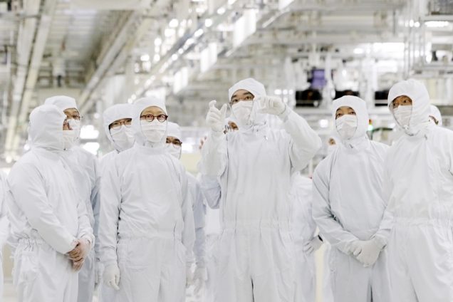
Intel was the first to commercialize backside power. However, Intel’s PowerVia took a route that involved changing the existing cell configuration, including adjusting pin counts and loosening wiring spacing during the test stage, effectively redesigning the cell structure. Samsung Electronics is also known to be pushing to introduce backside power in its 2-nanometer-class process, and it may take a direction similar to Intel’s.
Even with the same technology, the approaches diverge here. A method that rebuilds the cell can improve power efficiency, but it requires customers to redesign their chips. TSMC’s approach, which preserves the existing structure, reduces migration costs for customers and is seen as advantageous in retaining large clients with accumulated design assets.
An industry source said, “This achievement is a technology that can improve efficiency while reducing design burdens in products that need both power and performance, such as AI accelerators.” The source added, “In the Angstrom era, competition is intensifying on both process technology and the design ecosystem.”
The challenge for Korea’s semiconductor industry lies in the same point. Foundry competition is shifting beyond a simple fight over circuit widths to a battle over how easily customers’ design assets can be accepted.
For Samsung Electronics, the key to catching up is not only completing backside power technology, but also speeding up ecosystem improvements such as design tools and cell libraries. Some observers say now, while AI chip orders are pouring in, is the window of opportunity to narrow the gap.