The research team at the Massachusetts Institute of Technology (MIT) in the United States has developed an autonomous robotic system that measures the photoconductivity properties of semiconductor materials automatically. It is capable of performing over 3,000 precise measurements daily without human intervention.
The system was established by Professor Tonio Buonassisi’s research team in the Department of Mechanical Engineering at MIT. It operates continuously for 24 hours, measuring photoconductivity properties more than 125 times per hour. This approach is more accurate and faster than traditional manual methods or existing AI-based equipment.
Photoconductivity represents how well a semiconductor generates or transmits electricity when exposed to light. The values are a key performance indicator used in various clean energy technologies, including solar panels. It is especially important for evaluating the efficiency of new-generation solar cell materials, such as the currently popular perovskite.
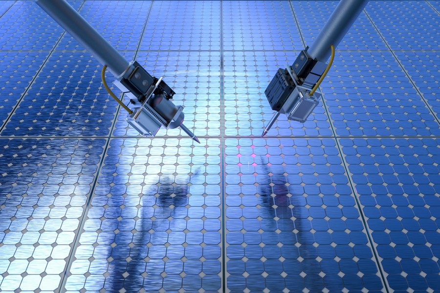
The robotic system captures sample images and uses image processing technology to divide the material surface into multiple zones. It then employs an artificial neural network model to calculate the optimal contact points for the probe. The neural network incorporates domain knowledge from material scientists, allowing it to learn and make decisions independently without labeled large-scale data.
The paths between measurement points are automatically calculated to be the shortest. To enhance movement efficiency, a small amount of randomness is applied to the algorithm. Through this process, the robot can quickly and stably conduct sequential measurements on multiple points.
The research team conducted comparative experiments with seven existing AI-based systems. The MIT system demonstrated higher efficiency in both measurement site selection and path planning. In practice, it performed over 3,000 measurements in a single day, accurately identifying areas of high photoconductivity and material degradation.
Moreover, the probe can be applied to various forms of samples, such as dots, droplets, and amorphous structures, increasing the versatility of automated experiments.
The research received support from First Solar, Eni, MathWorks, the University of Toronto Acceleration Consortium, the U.S. Department of Energy, and the National Science Foundation (NSF). The findings were published in the international journal “Science Advances.”
MIT researchers aim to further develop the autonomous measurement system to create a fully automated laboratory for the entire process of developing new semiconductor materials.